- 您现在的位置:买卖IC网 > Sheet目录3889 > PIC18C452T-E/L (Microchip Technology)IC MCU OTP 16KX16 A/D 44PLCC
186
8197C–AVR–05/11
ATtiny261A/461A/861A
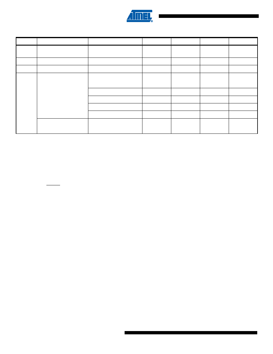
Notes:
1. Typical values at +25
°C.
2. “Min” means the lowest value where the pin is guaranteed to be read as high.
3. “Max” means the highest value where the pin is guaranteed to be read as low.
4. Although each I/O port can sink more than the test conditions (10 mA at V
CC = 5V, 5 mA at VCC = 3V) under steady state
conditions (non-transient), the sum of all IOL (for all ports) should not exceed 100 mA. If IOL exceeds the test conditions, VOL
may exceed the related specification. Pins are not guaranteed to sink current greater than the listed test condition.
5. Although each I/O port can source more than the test conditions (10 mA at V
CC = 5V, 5 mA at VCC = 3V) under steady state
conditions (non-transient), the sum of all IOH (for all ports) should not exceed 100 mA. If IOH exceeds the test condition, VOH
may exceed the related specification. Pins are not guaranteed to source current greater than the listed test condition.
6. The RESET pin must tolerate high voltages when entering and operating in programming modes and, as a consequence,
has a weak drive strength as compared to regular I/O pins. See Figure 20-32, Figure 20-33, Figure 20-34, and Figure 20-35
(starting on page 214).
7. Values are with external clock using methods described in “Minimizing Power Consumption” on page 37. Power Reduction is
enabled (PRR = 0xFF) and there is no I/O drive.
8. BOD Disabled.
IIH
Input Leakage
Current I/O Pin
VCC = 5.5V, pin high
(absolute value)
< 0.05
1
A
RRST
Reset Pull-up Resistor
30
60
k
Ω
RPU
I/O Pin Pull-up Resistor
20
50
k
Ω
ICC
Power Supply Current (7)
Active 1MHz, VCC = 2V
0.2
0.5
mA
Active 4MHz, VCC = 3V
1.2
2
mA
Active 8MHz, VCC = 5V
3.6
7
mA
Idle 1MHz, VCC = 2V
0.04
0.15
mA
Idle 4MHz, VCC = 3V
0.25
0.4
mA
Idle 8MHz, VCC = 5V
0.9
1.5
mA
Power-down mode (8)
WDT enabled, VCC = 3V
4
10
A
WDT disabled, VCC = 3V
0.15
2
A
Table 19-1.
DC Characteristics. T
A = -40°C to +85°C, VCC = 1.8V to 5.5V (unless otherwise noted).
Symbol
Parameter
Condition
Min
Typ(1)
Max
Units
发布紧急采购,3分钟左右您将得到回复。
相关PDF资料
PIC16C54C-40/SS
IC MCU OTP 512X12 20SSOP
22-15-3033
CONN FFC/FPC 3POS .100 RT ANG
PIC18LC858T-I/PT
IC MCU OTP 16KX16 CAN 80TQFP
22-02-3033
CONN FFC/FPC VERTICAL 3POS .100
PIC18C858T-E/PT
IC MCU OTP 16KX16 CAN 80TQFP
PIC18C858T-I/PT
IC MCU OTP 16KX16 CAN 80TQFP
PIC18C658T-I/PT
IC MCU OTP 16KX16 CAN 64TQFP
PIC16LC717T-E/SS
IC MCU OTP 2KX14 A/D PWM 20SSOP
相关代理商/技术参数
PIC18C452T-E/PT
功能描述:8位微控制器 -MCU 32KB 1536 RAM 34I/O RoHS:否 制造商:Silicon Labs 核心:8051 处理器系列:C8051F39x 数据总线宽度:8 bit 最大时钟频率:50 MHz 程序存储器大小:16 KB 数据 RAM 大小:1 KB 片上 ADC:Yes 工作电源电压:1.8 V to 3.6 V 工作温度范围:- 40 C to + 105 C 封装 / 箱体:QFN-20 安装风格:SMD/SMT
PIC18C452T-I/L
功能描述:8位微控制器 -MCU 32KB 1536 RAM 34I/O RoHS:否 制造商:Silicon Labs 核心:8051 处理器系列:C8051F39x 数据总线宽度:8 bit 最大时钟频率:50 MHz 程序存储器大小:16 KB 数据 RAM 大小:1 KB 片上 ADC:Yes 工作电源电压:1.8 V to 3.6 V 工作温度范围:- 40 C to + 105 C 封装 / 箱体:QFN-20 安装风格:SMD/SMT
PIC18C452T-I/PT
功能描述:8位微控制器 -MCU 32KB 1536 RAM 34I/O RoHS:否 制造商:Silicon Labs 核心:8051 处理器系列:C8051F39x 数据总线宽度:8 bit 最大时钟频率:50 MHz 程序存储器大小:16 KB 数据 RAM 大小:1 KB 片上 ADC:Yes 工作电源电压:1.8 V to 3.6 V 工作温度范围:- 40 C to + 105 C 封装 / 箱体:QFN-20 安装风格:SMD/SMT
PIC18C601-I/L
功能描述:8位微控制器 -MCU 256KB 1536 RAM 26I/O RoHS:否 制造商:Silicon Labs 核心:8051 处理器系列:C8051F39x 数据总线宽度:8 bit 最大时钟频率:50 MHz 程序存储器大小:16 KB 数据 RAM 大小:1 KB 片上 ADC:Yes 工作电源电压:1.8 V to 3.6 V 工作温度范围:- 40 C to + 105 C 封装 / 箱体:QFN-20 安装风格:SMD/SMT
PIC18C601-I/L021
制造商:Microchip Technology Inc 功能描述:
PIC18C601-I/PT
功能描述:8位微控制器 -MCU 256KB 1536 RAM 26I/O RoHS:否 制造商:Silicon Labs 核心:8051 处理器系列:C8051F39x 数据总线宽度:8 bit 最大时钟频率:50 MHz 程序存储器大小:16 KB 数据 RAM 大小:1 KB 片上 ADC:Yes 工作电源电压:1.8 V to 3.6 V 工作温度范围:- 40 C to + 105 C 封装 / 箱体:QFN-20 安装风格:SMD/SMT
PIC18C601T-I/L
功能描述:8位微控制器 -MCU 256KB 1536 RAM 26I/O RoHS:否 制造商:Silicon Labs 核心:8051 处理器系列:C8051F39x 数据总线宽度:8 bit 最大时钟频率:50 MHz 程序存储器大小:16 KB 数据 RAM 大小:1 KB 片上 ADC:Yes 工作电源电压:1.8 V to 3.6 V 工作温度范围:- 40 C to + 105 C 封装 / 箱体:QFN-20 安装风格:SMD/SMT
PIC18C601T-I/PT
功能描述:8位微控制器 -MCU 256KB 1536 RAM 26I/O RoHS:否 制造商:Silicon Labs 核心:8051 处理器系列:C8051F39x 数据总线宽度:8 bit 最大时钟频率:50 MHz 程序存储器大小:16 KB 数据 RAM 大小:1 KB 片上 ADC:Yes 工作电源电压:1.8 V to 3.6 V 工作温度范围:- 40 C to + 105 C 封装 / 箱体:QFN-20 安装风格:SMD/SMT